XANTAR® LDS
Diversification, styling, miniaturization and cost reduction are trends in portable electronics. LDS is becoming increasingly popular as the MID technology to enable an increased number of novel functions available inside appealing housings and covers, such as smart phones and notebooks. With LDS, tailored plastic materials are activated locally using a laser, and subsequently metalized exclusively in the activated areas, thus enabling a fast, highly flexible and 3D-design of for instance antennas in existing parts such as covers and frames.
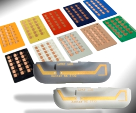
The XANTAR LDS portfolio is ideally suited for integrated mobile phone antennas from antenna carriers to fully integrated antennas in the housing or frame. Over the last years, the application area has now been extended to antennas in laptops, notebooks, tablets, POS applications and smart watches. Furthermore, LDS has found its commercially employed way into automotive & mobility industry, as well as lighting and medical applications.
Full Colour custom-made PC- and PC/ABS-based grades are available that enable selective electroless plating by means of laser direct structuring (LDS) to integrate electric circuits into moulded parts. For parts that require soldering, mature low temperature soldering solutions are employed successfully in industry over a larger number of years.
Optimized for LDS technology:
- Highest-impact material available for laser direct structuring
- Halogen free flame retardant
- Resolution (line/space) down to 100 microns
- Extremely well suited for antennas in mobile phones and notebooks
- Full colour availability for PC- and PC/ABS based LDS grades
High-performance/robustness:
- Dielectric constant of PC/ABS helps to assure high antenna performance
- Outstanding impact strength outperforms competitive PC-blends
Advantages of innovative LDS technology:
- Higher flexibility compared to other moulded interconnect device (MID) technologies, providing faster time-to-market
- Enables 3D shapes and electrical connections simultaneously
- Suitable for relatively small surface areas
- Only three process steps: moulding, laser processing, metallization